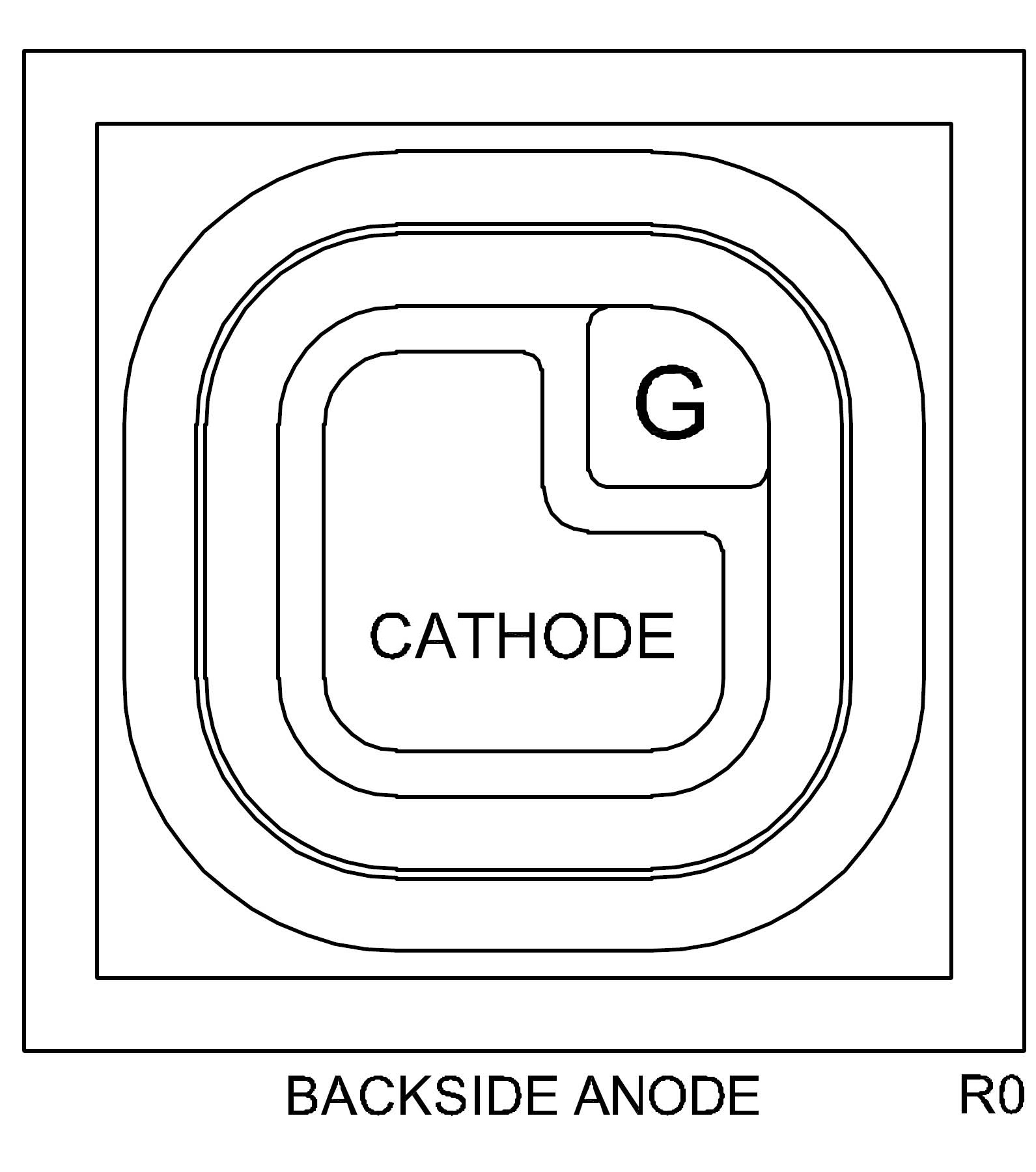
Technical Specifications
Similar Products with Selected SpecificationsTest Conditions
ITM = 1 A
tp = 380 µs
Test Conditions
VD = 12 V
Test Conditions
VD = 12 V
Test Conditions
IT = 100 mA
RGK = 1 kΩ
Test Conditions
VDRM = 400 V
RGK = 1 kΩ
Test Conditions
VDRM = 400 V
RGK = 1 kΩ
TC = 125 °C
Test Conditions
VD = 267 V
RGK = 1 kΩ
TC = 125 °C
Test Conditions
VRRM = 400 V
RGK = 1 kΩ
Test Conditions
VRRM = 400 V
RGK = 1 kΩ
TC = 125 °C
Ordering
| Part | Package | Buy | Status | Description | ECCN Code | HTS Code | Termination |
|---|---|---|---|---|---|---|---|
| CPS053-CS92D-CM | WafflePack@400 | Active | .8A,400V Bare die,53.150 X 53.150 mils,SCR | EAR99 | 8541.30.0040 | PBFREE | |
| CPS053-CS92D-CT | WafflePack@400 | Active | .8A,400V Bare die,53.150 X 53.150 mils,SCR | EAR99 | 8541.30.0040 | PBFREE | |
| CPS053-CS92D-CT20 | WafflePack@20 | Special Order Item | .8A,400V Bare die,53.150 X 53.150 mils,SCR | EAR99 | 8541.30.0040 | PBFREE |
Resources
| Item | Type |
|---|---|
| No matching documents found. | |
| Analytical Test Report:Active Device, Rectifier | Analytical Test Report |
| Analytical Test Report:Die | Analytical Test Report |
| Analytical Test Report:Die | Analytical Test Report |
| Analytical Test Report:Wafer Schottky | Analytical Test Report |
| Analytical Test Report:Wafer Schottky | Analytical Test Report |
| Analytical Test Report:Wafer Switching Diode | Analytical Test Report |
| Analytical Test Report:Wafer Transistor | Analytical Test Report |
| Analytical Test Report:Wafer Zener | Analytical Test Report |
| Analytical Test Report:Wafer/Die | Analytical Test Report |
| CPS053-CS92D_WPD.PDF | Device Datasheet |
| Package Detail Document:WAFER | Package Detail Document |