CP191V-H2N2222A-CM
40V,800mA,500mW Bare die,16.535 X 16.535 mils,Transistor-Small Signal (<=1A)
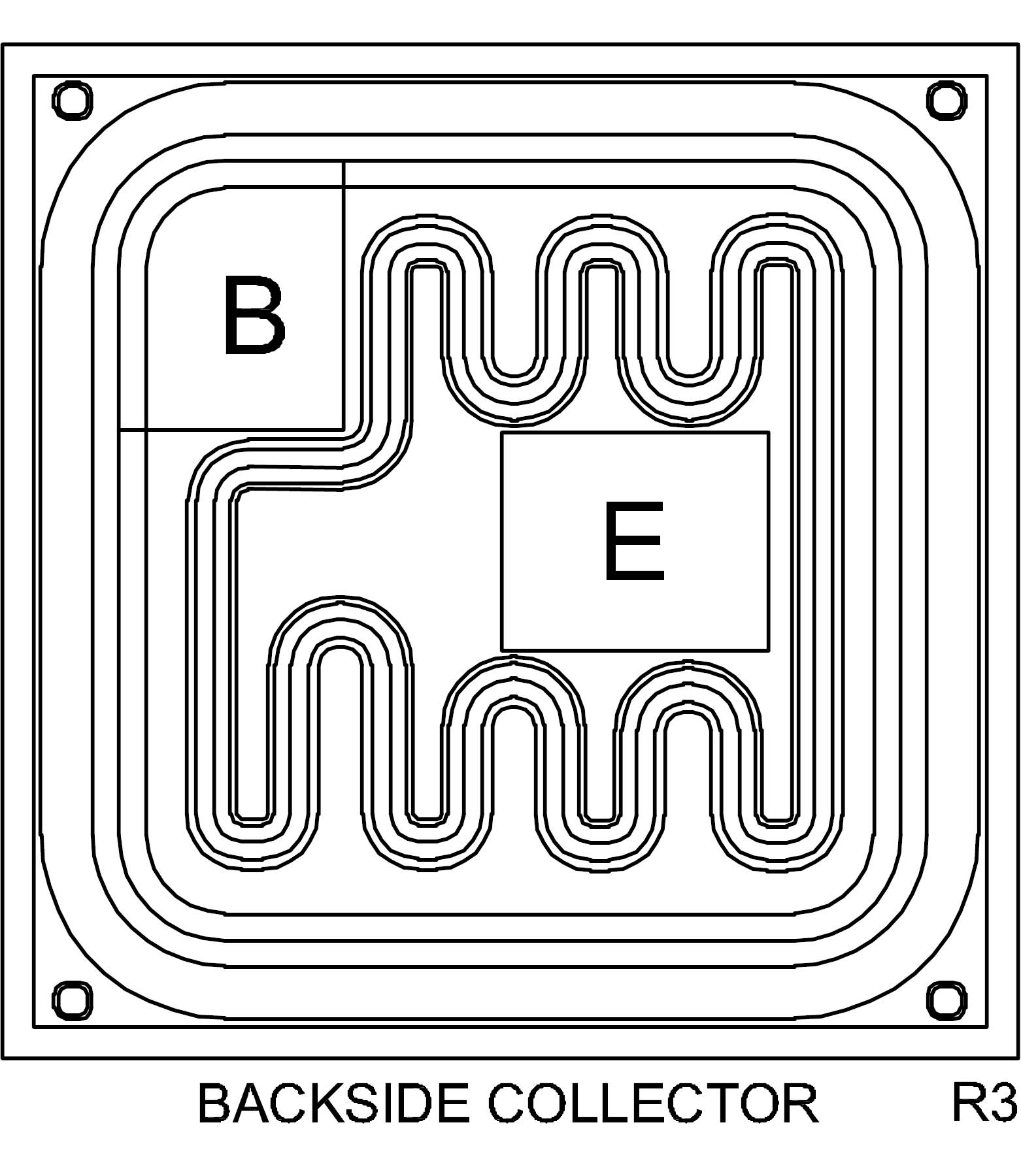
Case Type: CHIP,WAFFLE
Technical Specifications
Similar Products with Selected SpecificationsTest Conditions
IC = 150 mA
IB = 15 mA
Test Conditions
IC = 500 mA
IB = 50 mA
Test Conditions
IC = 10 µA
Test Conditions
VCB = 60 V
Test Conditions
VCB = 60 V
TA = 150 °C
Test Conditions
VCB = 10 V
f = 31.8 MHz
IE = 20 mA
Test Conditions
IC = 10 mA
Test Conditions
VCE = 60 V
VBE(OFF) = 3 V
Test Conditions
IC = 150 mA
IB = 15 mA
Test Conditions
IC = 500 mA
IB = 50 mA
Test Conditions
VCE = 20 V
IC = 20 mA
f = 100 MHz
Test Conditions
VCE = 10 V
IC = 100 µA
Test Conditions
VCE = 10 V
IC = 1 mA
Test Conditions
VCE = 10 V
IC = 10 mA
Test Conditions
VCE = 10 V
IC = 10 mA
TA = -55 °C
Test Conditions
VCE = 10 V
IC = 150 mA
Test Conditions
VCE = 1 V
IC = 150 mA
Test Conditions
VCE = 10 V
IC = 500 mA
Test Conditions
VCC = 30 V
IC = 150 mA
IB1 = 15 mA
VBE = 0.5 V
Test Conditions
IE = 10 µA
Test Conditions
VEB = 3 V
Test Conditions
VCC = 30 V
IC = 150 mA
IB1 = 15 mA
IB2 = 15 mA
Test Conditions
VEB = 0.5 V
f = 100 kHz
Test Conditions
VCE = 10 V
IC = 1 mA
f = 1 kHz
Test Conditions
VCE = 10 V
IC = 10 mA
f = 1 kHz
Test Conditions
VCE = 10 V
IC = 100 µA
f = 1 kHz
RS = 1 kΩ
Test Conditions
VCE = 10 V
IC = 1 mA
f = 1 kHz
Test Conditions
VCE = 10 V
IC = 10 mA
f = 1 kHz
Test Conditions
VCB = 10 V
f = 100 kHz
Test Conditions
VCC = 30 V
IC = 150 mA
IB1 = 15 mA
VBE = 0.5 V
Test Conditions
VCE = 10 V
IC = 1 mA
f = 1 kHz
Test Conditions
VCE = 10 V
IC = 10 mA
f = 1 kHz
Test Conditions
VCC = 30 V
IC = 150 mA
IB1 = 15 mA
IB2 = 15 mA
Test Conditions
VCE = 10 V
IC = 1 mA
f = 1 kHz
Test Conditions
VCE = 10 V
IC = 10 mA
f = 1 kHz
Ordering
| Part | Package | Buy | Status | Description | ECCN Code | HTS Code | Termination |
|---|---|---|---|---|---|---|---|
| CP191V-H2N2222A-CM | WafflePack@400 | Active | 40V,800mA,500mW Up-Screened Bare Die MIL-PRF-38534 Class H Equivalent,16.535 X 16.535 mils,Transistor-Small Signal (<=1A) | EAR99 | 8541.21.0040 | PBFREE |
Resources
| Item | Type |
|---|---|
| No matching documents found. | |
| Analytical Test Report:Active Device, Rectifier | Analytical Test Report |
| Analytical Test Report:Die | Analytical Test Report |
| Analytical Test Report:Die | Analytical Test Report |
| Analytical Test Report:Wafer Schottky | Analytical Test Report |
| Analytical Test Report:Wafer Schottky | Analytical Test Report |
| Analytical Test Report:Wafer Switching Diode | Analytical Test Report |
| Analytical Test Report:Wafer Transistor | Analytical Test Report |
| Analytical Test Report:Wafer Zener | Analytical Test Report |
| Analytical Test Report:Wafer/Die | Analytical Test Report |
| CP191V-2N2222A_WPD.PDF | Device Datasheet |
| Package Detail Document:WAFER | Package Detail Document |
| Process Change Notice:CP191V / CP591X Wafers | Process Change Notice |
| Spice Model:Spice Model CP191V | Spice Model |