BAW101
200mA,300V Surface mount Diode-Switching Dual: High Voltage: Same Polarity
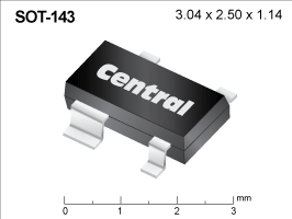
Case Type: SOT-143
Technical Specifications
Similar Products with Selected SpecificationsTest Conditions
IF = 100 mA
(0.9 V Typical)
Test Conditions
f = 1 MHz
Test Conditions
IR = 100 µA
Test Conditions
IF = 30 mA
IR = 30 mA
IREC = 3 mA
RL = 100 Ω
Test Conditions
VR = 250 V
Test Conditions
VR = 250 V
TA = 150 °C
Ordering
| Part | Package | Buy | Status | Description | ECCN Code | HTS Code | Termination |
|---|---|---|---|---|---|---|---|
| BAW101 TR | Tape & Reel@3,000 | Discontinued | 200mA,300V Surface mount Diode-Switching Dual: High Voltage: Same Polarity | EAR99 | 8541.10.0070 | PBFREE |
Resources
| Item | Type |
|---|---|
| No matching documents found. | |
| Analytical Test Report:Alloy 42 leadframe | Analytical Test Report |
| Analytical Test Report:Die Attach | Analytical Test Report |
| Analytical Test Report:Epoxy Adhesive | Analytical Test Report |
| Analytical Test Report:Halogen Free | Analytical Test Report |
| Analytical Test Report:Pure Tin Solder, Sn | Analytical Test Report |
| BAW101.PDF | Device Datasheet |
| Material Composition:SOT-143 | Material Composition |
| Package Detail Document:SOT-143 | Package Detail Document |
| Process Change Notice:BAW101 Alternate Marking | Process Change Notice |
| Product EOL Notice:BAW101 | Product EOL Notice |
| Step File 3D Object:SOT-143 (TO-253AA) | Step File 3D Object |