CTLDM7181-M832D
Surface mount MOSFET 1A,20V Dual: N-Channel/P-Channel MOSFET&860mA,20V
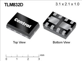
Case Type: TLM832D
Technical Specifications
Similar Products with Selected SpecificationsTest Conditions
VDS = 10 V
f = 1 MHz
Test Conditions
VDS = 16 V
f = 1 MHz
Test Conditions
VDS = 10 V
f = 1 MHz
Test Conditions
VDS = 16 V
f = 1 MHz
Test Conditions
VDS = 10 V
f = 1 MHz
Test Conditions
VDS = 16 V
f = 1 MHz
Test Conditions
IS = 1 A
Test Conditions
IS = 360 mA
Test Conditions
ID = 250 µA
Test Conditions
ID = 250 µA
(24 V Typical)
Test Conditions
VDS = 10 V
ID = 500 mA
Test Conditions
VDS = 10 V
ID = 810 mA
Test Conditions
VGS = 8 V
Test Conditions
VGS = 8 V
(0.001 µA Typical)
Test Conditions
VGS = 8 V
Test Conditions
VGS = 8 V
(0.001 µA Typical)
Test Conditions
ID = 1 mA
VDS = 10 V
Test Conditions
ID = 250 µA
(0.76 V Typical)
Test Conditions
VDS = 10 V
VGS = 4.5 V
ID = 1 A
Test Conditions
VDS = 10 V
VGS = 4.5 V
ID = 1 A
Test Conditions
VDS = 10 V
VGS = 4.5 V
ID = 1 A
Test Conditions
VDS = 10 V
VGS = 4.5 V
ID = 1 A
Test Conditions
VDS = 20 V
(0.005 µA Typical)
Test Conditions
VDS = 20 V
Test Conditions
VGS = 4.5 V
ID = 500 mA
(75 mΩ Typical)
Test Conditions
VGS = 2.5 V
ID = 500 mA
(100 mΩ Typical)
Test Conditions
VGS = 1.5 V
ID = 100 mA
(170 mΩ Typical)
Test Conditions
VGS = 4.5 V
ID = 950 mA
(85 mΩ Typical)
Test Conditions
VGS = 4.5 V
ID = 770 mA
(85 mΩ Typical)
Test Conditions
VGS = 2.5 V
ID = 670 mA
(130 mΩ Typical)
Test Conditions
VGS = 1.8 V
ID = 200 mA
(190 mΩ Typical)
Test Conditions
VDS = 10 V
VGS = 4.5 V
ID = 1 A
Test Conditions
VDS = 10 V
VGS = 4.5 V
ID = 1 A
Test Conditions
VDD = 10 V
ID = 500 mA
VGS = 5 V
Test Conditions
VDD = 10 V
ID = 950 mA
RG = 6 Ω
VGS = 4.5 V
Test Conditions
VDD = 10 V
ID = 500 mA
VGS = 5 V
Test Conditions
VDD = 10 V
RG = 6 Ω
ID = 950 mA
VGS = 4.5 V
Ordering
| Part | Package | Buy | Status | Description | ECCN Code | HTS Code | Termination |
|---|---|---|---|---|---|---|---|
| CTLDM7181-M832D TR | Tape & Reel@3,000 | Discontinued | Surface mount MOSFET 1A,20V Dual: N-Channel/P-Channel MOSFET&860mA,20V | EAR99 | 8541.29.0055 | PBFREE |
Resources
| Item | Type |
|---|---|
| No matching documents found. | |
| Analytical Test Report:Die Attach | Analytical Test Report |
| Analytical Test Report:Die Attach | Analytical Test Report |
| Analytical Test Report:Gold Bond Wire | Analytical Test Report |
| Analytical Test Report:Green Epoxy Molding Compound | Analytical Test Report |
| CTLDM7181-M832D.PDF | Device Datasheet |
| Package Detail Document:TLM832D | Package Detail Document |
| Process Change Notice:TLM832D Leadframe change from | Process Change Notice |
| Product EOL Notice:BLANKET PDN-ALL OTHER PRODUCTS | Product EOL Notice |