CWDM408P8N
13.5A,40V Surface mount MOSFET N-Channel Enhancement Mode High Current
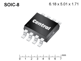
Case Type: SOIC-8
Technical Specifications
Similar Products with Selected SpecificationsTest Conditions
IS = 1 A
Test Conditions
ID = 250 µA
Test Conditions
VGS = 20 V
Test Conditions
VGS = 20 V
Test Conditions
ID = 250 µA
VDS = 40 V
(1.4 V Typical)
Test Conditions
VDS = 40 V
Test Conditions
VGS = 10 V
ID = 1 A
(4 mΩ Typical)
Test Conditions
VGS = 4.5 V
ID = 1 A
(5.6 mΩ Typical)
Ordering
| Part | Package | Buy | Status | Description | ECCN Code | HTS Code | Termination |
|---|---|---|---|---|---|---|---|
| CWDM408P8N BK | Box@350 | Special Order Item | 13.5A,40V Surface mount MOSFET N-Channel Enhancement Mode High Current | EAR99 | 8541.21.0095 | PBFREE | |
| CWDM408P8N TR13 | Tape & Reel@2,500 | Special Order Item | 13.5A,40V Surface mount MOSFET N-Channel Enhancement Mode High Current | EAR99 | 8541.21.0095 | PBFREE |
Resources
| Item | Type |
|---|---|
| No matching documents found. | |
| Analytical Test Report:Die Attach | Analytical Test Report |
| Analytical Test Report:Epoxy Molding Compound | Analytical Test Report |
| Analytical Test Report:Lead frame | Analytical Test Report |
| Analytical Test Report:Wire | Analytical Test Report |
| Material Composition:SOIC-8 | Material Composition |
| Package Detail Document:SOIC-8 | Package Detail Document |
| Product Reliability Data:SOIC-8 Package Reliability | Product Reliability Data |