MPSA63
500mA,30V Through-Hole Transistor-Small Signal (<=1A) PNP Darlington
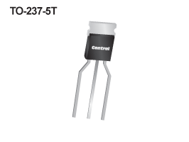
Case Type: TO-92
Technical Specifications
Similar Products with Selected SpecificationsTest Conditions
IC = 100 mA
VCE = 5 V
Test Conditions
VCB = 30 V
Test Conditions
IC = 100 µA
Test Conditions
IC = 100 mA
IB = 100 µA
Test Conditions
VCE = 5 V
IC = 100 mA
f = 100 MHz
Test Conditions
VCE = 5 V
IC = 10 mA
Test Conditions
VCE = 5 V
IC = 100 mA
Test Conditions
VEB = 10 V
Test Conditions
VCE = 5 V
IC = 1 mA
f = 1 kHz
RS = 100 kΩ
Test Conditions
VCB = 10 V
f = 100 kHz
Ordering
| Part | Package | Buy | Status | Description | ECCN Code | HTS Code | Termination |
|---|---|---|---|---|---|---|---|
| MPSA63 APM | Ammo@2,000 | Active | 500mA,30V Through-Hole Transistor-Small Signal (<=1A) PNP Darlington | EAR99 | 8541.21.0075 | LEAD or TIN | |
| MPSA63 APP | Ammo@2,000 | Active | 500mA,30V Through-Hole Transistor-Small Signal (<=1A) PNP Darlington | EAR99 | 8541.21.0075 | LEAD or TIN | |
| MPSA63 TRA | Tape & Reel@2,000 | Active | 500mA,30V Through-Hole Transistor-Small Signal (<=1A) PNP Darlington | EAR99 | 8541.21.0075 | LEAD or TIN | |
| MPSA63 TRE | Tape & Reel@2,000 | Active | 500mA,30V Through-Hole Transistor-Small Signal (<=1A) PNP Darlington | EAR99 | 8541.21.0075 | LEAD or TIN |
Resources
| Item | Type |
|---|---|
| No matching documents found. | |
| MPSA62-66.PDF | Device Datasheet |
| Package Detail Document:TO-237 | Package Detail Document |
| Product EOL Notice:TO-237 Transisitors | Product EOL Notice |