2N2368
15V,200mA,.36W Through-Hole Transistor-Small Signal (<=1A) NPN Saturated Switch
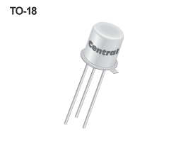
Case Type: TO-18
Technical Specifications
Similar Products with Selected SpecificationsTest Conditions
IC = 10 mA
IB = 1 mA
Test Conditions
IC = 10 µA
Test Conditions
VCB = 20 V
Test Conditions
VCB = 20 V
TA = 150 °C
Test Conditions
IC = 10 mA
Test Conditions
IC = 10 µA
Test Conditions
IC = 10 mA
IB = 1 mA
Test Conditions
VCE = 10 V
IC = 10 mA
f = 100 MHz
Test Conditions
VCE = 1 V
IC = 10 mA
Test Conditions
VCE = 1 V
IC = 10 mA
TA = -55 °C
Test Conditions
VCE = 2 V
IC = 100 mA
Test Conditions
IE = 10 µA
Test Conditions
VCB = 5 V
f = 140 kHz
Test Conditions
VCC = 3 V
IC = 10 mA
IB1 = 3 mA
IB2 = 1.5 mA
Test Conditions
VCC = 3 V
IC = 10 mA
IB1 = 3 mA
IB2 = 1.5 mA
Ordering
| Part | Package | Buy | Status | Description | ECCN Code | HTS Code | Termination |
|---|---|---|---|---|---|---|---|
| 2N2368 | Box@2,000 | Discontinued | 15V,200mA,.36W Through-Hole Transistor-Small Signal (<=1A) NPN Saturated Switch | EAR99 | 8541.21.0075 | TIN |
Resources
| Item | Type |
|---|---|
| No matching documents found. | |
| Analytical Test Report:Bond Wire | Analytical Test Report |
| Analytical Test Report:Cap | Analytical Test Report |
| Analytical Test Report:Header | Analytical Test Report |
| Analytical Test Report:Header Assembly | Analytical Test Report |
| Analytical Test Report:Pure Tin Solder | Analytical Test Report |
| LSSGP055.PDF | Device Datasheet |
| Material Composition:TO-18 | Material Composition |
| Package Detail Document:TO-18 | Package Detail Document |
| Product EOL Notice:2N2368 | Product EOL Notice |
| Product Reliability Data:TO-18 Package Reliability | Product Reliability Data |