D41D1
30V,1A,6.25W Through-Hole Transistor-Bipolar Power (>1A) PNP General Purpose Amplifier/Switch
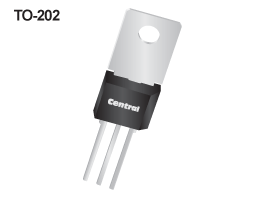
Case Type: TO-202
Technical Specifications
Similar Products with Selected SpecificationsTest Conditions
IC = 500 mA
IB = 50 mA
Test Conditions
IC = 10 mA
Test Conditions
VCE = 45 V
Test Conditions
IC = 500 mA
IB = 50 mA
Test Conditions
VCE = 2 V
IC = 100 mA
Test Conditions
VCE = 2 V
IC = 1 A
Test Conditions
VEB = 5 V
Ordering
| Part | Package | Buy | Status | Description | ECCN Code | HTS Code | Termination |
|---|---|---|---|---|---|---|---|
| D41D1 | Sleeve@50 | Discontinued | 30V,1A,6.25W Through-Hole Transistor-Bipolar Power (>1A) PNP General Purpose Amplifier/Switch | EAR99 | 8541.29.0055 | PBFREE |
Resources
| Item | Type |
|---|---|
| No matching documents found. | |
| Analytical Test Report:Bond Wire | Analytical Test Report |
| Analytical Test Report:Green Epoxy Molding Compound | Analytical Test Report |
| Analytical Test Report:Lead Frame | Analytical Test Report |
| Analytical Test Report:Tin Plating | Analytical Test Report |
| D41D_SERIES.PDF | Device Datasheet |
| Material Composition:TO-202 | Material Composition |
| Package Detail Document:TO-202 | Package Detail Document |
| Product EOL Notice:All Product in the TO-202 and | Product EOL Notice |
| Product Reliability Data:TO-202 Package Reliability | Product Reliability Data |