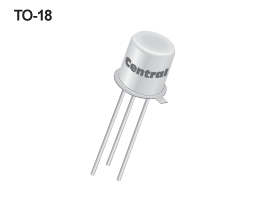
Technical Specifications
Similar Products with Selected SpecificationsTest Conditions
VGS = 10 V
f = 1 MHz
Test Conditions
VGS = 10 V
f = 1 MHz
Test Conditions
VDS = 15 V
VGS = 12 V
Test Conditions
VDS = 15 V
VGS = 12 V
TA = 150 °C
Test Conditions
f = 1 kHz
Test Conditions
ID = 10 mA
Test Conditions
VGS = 20 V
Test Conditions
VGS = 20 V
TA = 150 °C
Test Conditions
VDS = 15 V
ID = 1.5 µA
Test Conditions
VDS = 15 V
ID = 1 nA
Test Conditions
VDS = 15 V
Ordering
| Part | Package | Buy | Status | Description | ECCN Code | HTS Code | Termination |
|---|---|---|---|---|---|---|---|
| BSV79 | Box@2,000 | Discontinued | 2V,7V,50mA,350mW Through-Hole JFET N Channel | EAR99 | 8541.21.0095 | PBFREE |
Resources
| Item | Type |
|---|---|
| No matching documents found. | |
| Analytical Test Report:Bond Wire | Analytical Test Report |
| Analytical Test Report:Cap | Analytical Test Report |
| Analytical Test Report:Header | Analytical Test Report |
| Analytical Test Report:Header Assembly | Analytical Test Report |
| Analytical Test Report:Pure Tin Solder | Analytical Test Report |
| BSV79_80.PDF | Device Datasheet |
| Material Composition:TO-18 | Material Composition |
| Package Detail Document:TO-18 | Package Detail Document |
| Product EOL Notice:JFETS | Product EOL Notice |
| Product Reliability Data:TO-18 Package Reliability | Product Reliability Data |