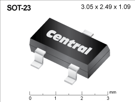
Technical Specifications
Similar Products with Selected SpecificationsTest Conditions
VGS = 20 V
Test Conditions
IG = 1 µA
Test Conditions
VDS = 15 V
ID = 10 nA
Test Conditions
VDS = 15 V
Test Conditions
VDS = 100 mV
Ordering
| Part | Package | Buy | Status | Description | ECCN Code | HTS Code | Termination |
|---|---|---|---|---|---|---|---|
| CMPFJ175 BK | Box@3,500 | Active | 3V,6V,50mA,225mW Surface mount JFET P Channel | EAR99 | 8541.21.0095 | PBFREE |
Resources
| Item | Type |
|---|---|
| No matching documents found. | |
| Analytical Test Report:Copper Bond Wire | Analytical Test Report |
| Analytical Test Report:Gold Bond Wire | Analytical Test Report |
| Analytical Test Report:Green Epoxy Molding Compound | Analytical Test Report |
| Analytical Test Report:Leadframe | Analytical Test Report |
| Analytical Test Report:Sn Plating | Analytical Test Report |
| CMPFJ175-176.PDF | Device Datasheet |
| Material Composition:SOT-23 | Material Composition |
| Package Detail Document:SOT-23 | Package Detail Document |
| Process Change Notice:Copper Wire Bonding | Process Change Notice |
| Process Change Notice:CP613V Replaces CP688 | Process Change Notice |
| Product Brief:PB JFETs | Product Brief |
| Product Reliability Data:SOT-23 Package Reliability | Product Reliability Data |
| Spice Model:CMPFJ175 | Spice Model |
| Step File 3D Object:SOT-23 | Step File 3D Object |
